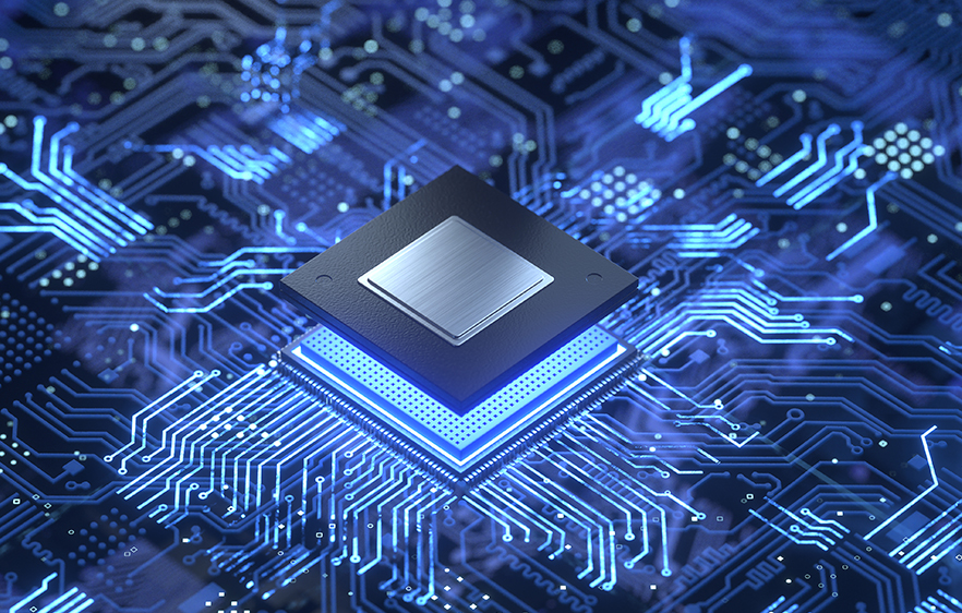
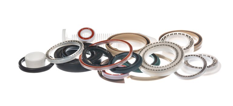
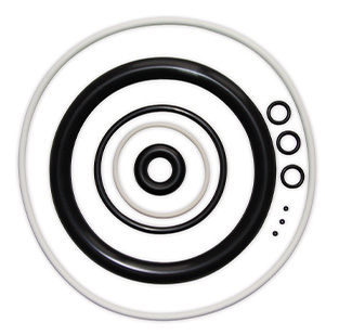
Seals for semiconductor applications
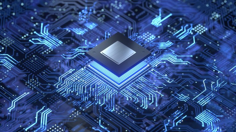
There are greater demands on semiconductor and electronics manufacturers for more complex and powerful devices to fulfil applications across all industry segments. High performance seals and ultra high purity elastomer materials are crucial for these critical applications.
Characteristics of semiconductor sealing
The technology push for more complex devices requires semiconductor companies to research and design new methods of processing within their manufacturing cells. This brings an increase in challenging technical conditions including complex chemistry, increased temperatures and stringent cleanliness within manufacturing process and the surrounding tools.
Component and material suppliers face these complex challenges daily. They must follow the same rules and ensure all criteria for new processes are fully met. Suppliers must also consider the combined effects of all the conditions outlined above.
Our world demands modern performance materials for the semiconductor industry. It’s therefore apparent materials previously formulated for older generation tools may not be technically capable in new and future applications. Therefore, it’s paramount to investigate and formulate new performance materials that meet each specific application.
Wet cleaning and ECD
Wet cleaning is a method used in semiconductor manufacturing to remove any contaminants from each layer of the wafer surface, usually by using chemicals and pure water. ECD is a method of laying down the bulk of the copper wiring within a semiconductor device.
Compounds for wet cleaning are engineered for static and dynamic applications with minimal metallic ion contamination.
Thermal applications
Compounds for these applications are required to have excellent thermal stability and maintain integrity at elevated temperatures often found in processes such as Oxidation, Diffusion, Annealing, and RTP.
These processes are extremely challenging for seal materials. High thermal load at 300°C with temperature cycling can encourage compression set, and they must also be manufactured to limit out-gassing at high temperature to prevent contamination within the process area and offer superior physical properties.
Thin film and dry etch
Thin film deposition is the process of creating and depositing thin film coatings onto a substrate material. These coatings can be made of many different materials, from metals to oxides to compounds. Dry etch is a process for material removal.
There are many Thin Film applications that present harsh plasma and gas environments, often at elevated temperatures. These include HDPCVD, PECVD, SACVD, PVD and ALD, along with Dry Etch and Ashing processes.
Whereas traditional seals might deteriorate and fail in these conditions, our next-generation compounds have excellent chemical and thermal resistance. Consequently, they are virtually impervious to extreme fabrication processes, therefore excellent for semiconductor seals.
Plasma processes are a very hostile and aggressive environment for seal materials. The corrosive chemistry at temperatures up to 250°C means compounds must be chemically and thermally stable across the operating range. Additionally, they must include low-outgassing and low particle count features. These applications are varied; from window and door seals, chamber lid seals, valve seals, and exhaust flange seals. They each require application knowledge to ensure all technical parameters are met before materials are recommended.
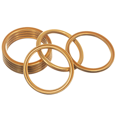
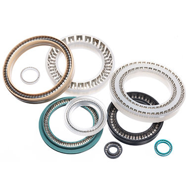
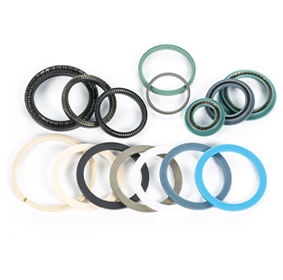
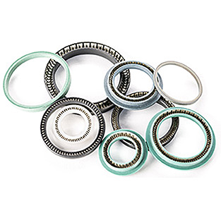
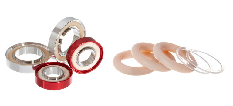
Ultra High Purity (UHP) materials
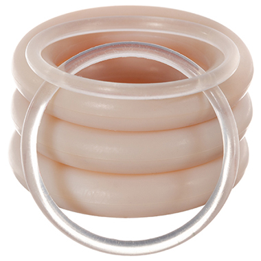
Perfluoroelastomer materials
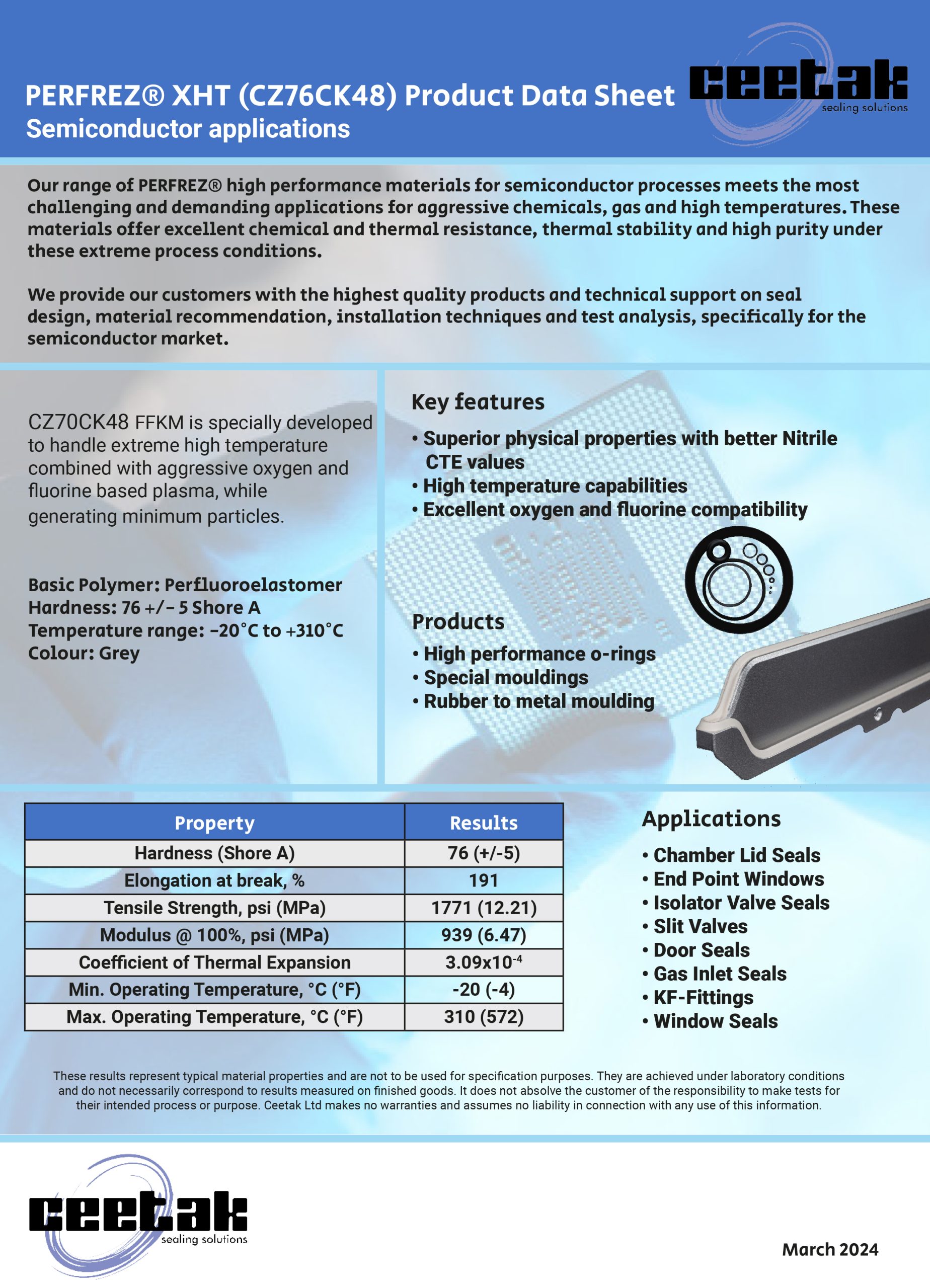
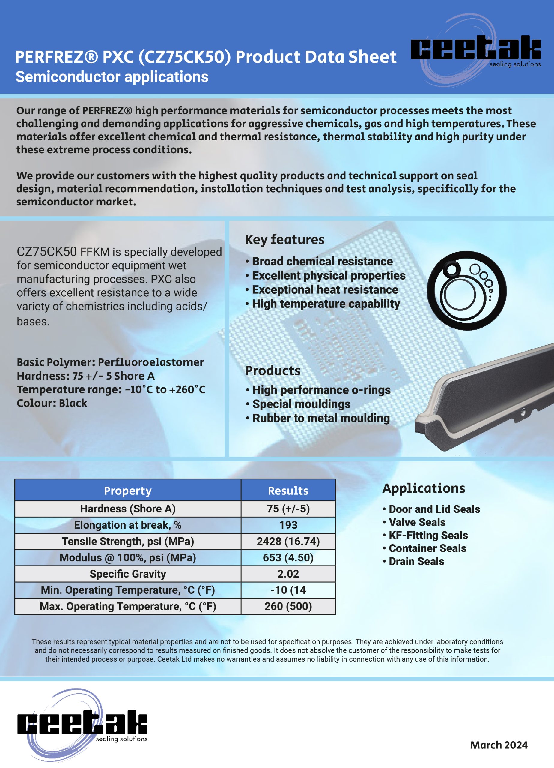
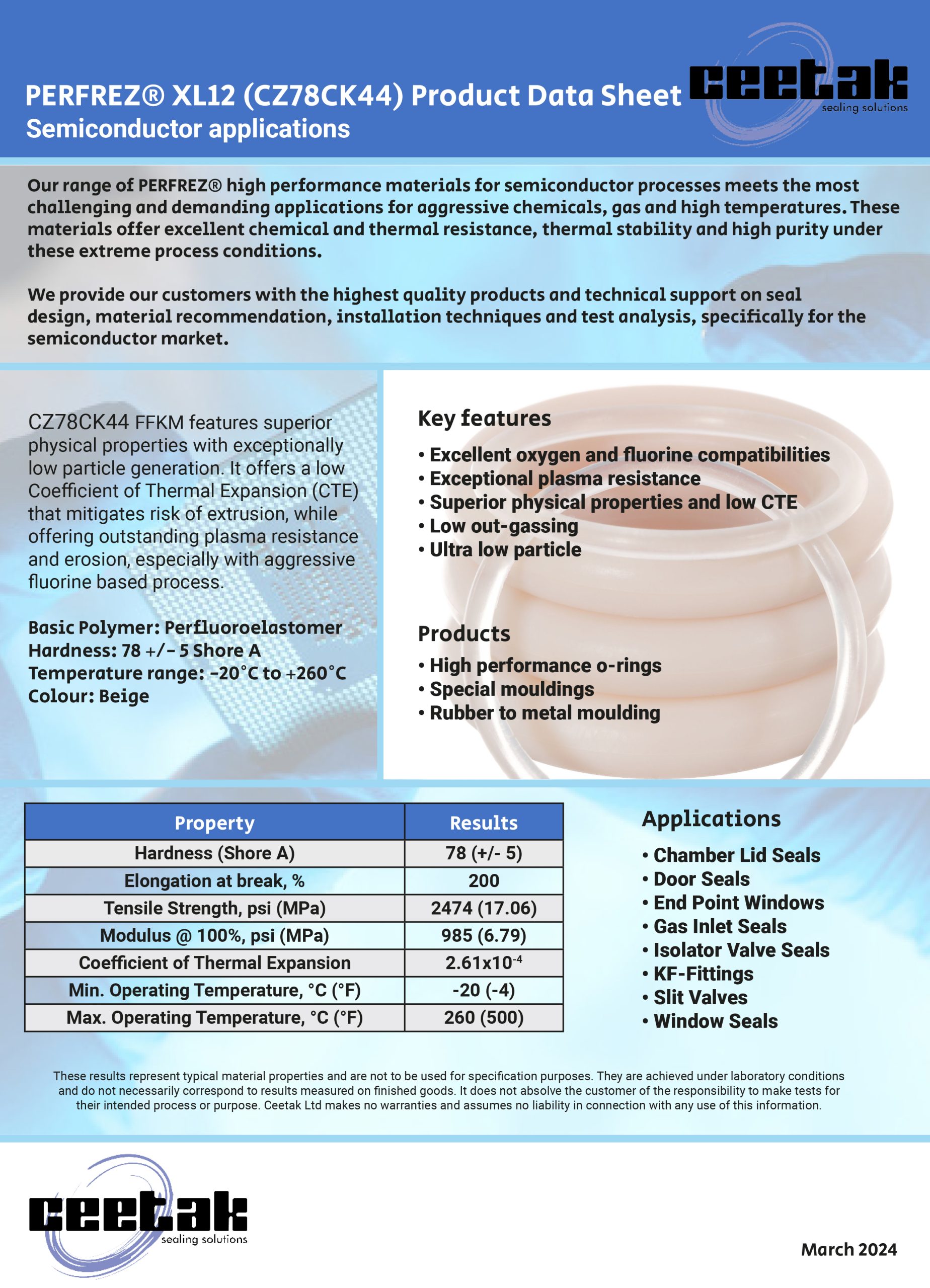
FFKM’s contain fully fluorinated polymer chains. Subsequently, FFKM elastomers deliver ultimate performance in multiple applications. These applications include where seals encounter high temperatures and aggressive chemicals for plasma, wet and dry, semiconductor process applications. There is an extensive range of FFKM materials available. The challenge lies in selecting the correct material grade for each application because no single perfluoroelastomer can meet all semiconductor process requirements. . For example, some materials are better than others at high temperatures, some demonstrate better chemical resistance and some are poor at thermal expansion.
Several compounds within our range of PERFREZ® perfluoroelastomer materials offer the best performance characteristics based on high thermal values, excellent low out-gassing and low particle count. We also offer a hybrid material which is an excellent “all-rounder” as it’s chemical formulation falls between FKM and FFKM. This means it performs consistently under slightly less demanding application conditions and with the added benefit of lower cost of purchase versus ultra-high grade FFKM’s.
Other compounds within our range are very specific to semiconductor process applications such as CVD, PVD, Plasma Etch (oxide & metal), fluorine and oxygen compatibility with a high temperature threshold material for sub-fab NW /ISO exhaust line environments. As new challenging processes emerge within the semiconductor industry, further progress in high temperature materials above 300° C will be developed. We expect to add a new generation material for plasma applications to our portfolio of materials by the end of 2022.
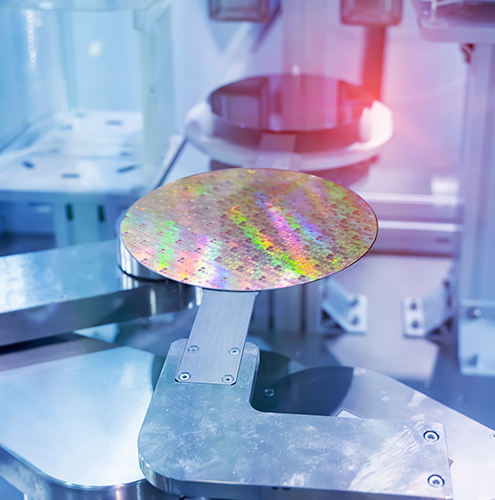
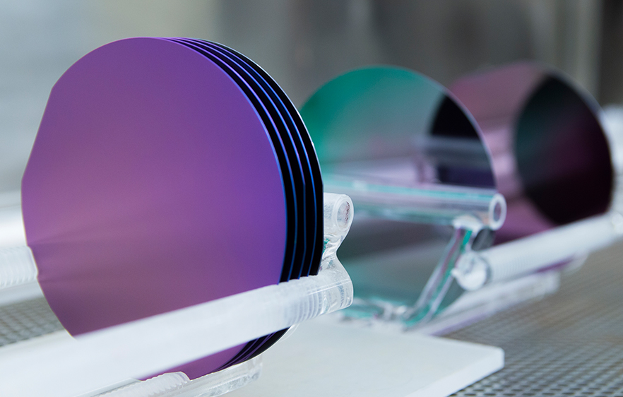
Cleanroom manufacturing
Semiconductor cleanrooms must be designed to control static, out-gassing, and any contamination. This includes external particulates such as dust, dirt, airborne microbes, and aerosol particles. Just a single particle of dust or debris on a wafer or component is enough to cause a catastrophic defect (that will ultimately lead to failure of a device).
Technicians create and maintain cleanrooms by removing the air and circulating it through a filtering system. The clean and filtered air back is distributed back into the cleanroom environment. Varying levels of cleanliness are possible. It depends on what is specified for each individual manufacturing environment or the finished product requirements. Different cleanliness levels are classified by the concentration of airborne particles within a measured space.
Bringing in any auxiliary products (such as seals) into the environment must also maintain the same levels of cleanliness.
We provide a complete cleanroom production process; from material blank production through to inspection and packaging using controlled materials within state-of-the-art cleanrooms. Our clean room manufacturing facilities are Class 7 (10,000) manufacturing and Class 5 (100) inspection, cleaning, & packaging.
Read more about our expertise in the semiconductor industry and how we can help you with your seals for semiconductor applications HERE